Introduction : processors and their role in digital technology
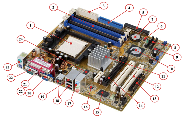
Computers, like all other digital equipment, are an assembly of several electronic components, for example :
- The circuit board, which connects the various components, coordinates tasks and allocates resources (Figure 1);
- The processor, which executes the tasks (number 1);
- The random access memory (or RAM), which stores information temporarily so that it can be accessed quickly by the processor (number 6);
- The hard disk, which stores all the data needed to run the computer and user data on a more permanent basis (numbers 4 and 5);
- The graphics processor, which processes graphics data so that it can be displayed. Its structure and composition are relatively similar to that of the processor (number 14).
What is a processor and how does it work ?
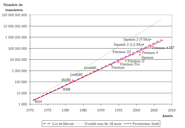
The processors we are interested in here are made up of smaller units called transistors. These transistors form logic circuits, which process the information passing through them in the form of electrical currents. The computing power of a processor is linked to the number of transistors it contains, a figure that increases with ever more advanced technologies. According to Moore's Law (Figure 2), the density of transistors on a chip is supposed to double every two years. This assumption proved to be relatively accurate for a few decades, but progress is being slowed down by physical constraints and the evolution of computing power is moving away from Moore's Law.
Transistors : the core of microchips
Two types of chips : logic and memory
The most common types of processors are "logic" chips and "memory" chips:
- Logic chips are the 'brains' of electronic devices, processing information to perform a task. They are essential to their operation because they provide the processing power needed by all digital devices, from servers to small connected objects.
- The second is data storage. There are two types: volatile memory, which is erased when the device is switched off (DRAM chips), and non-volatile memory, which is retained (NAND chips). For more details, see this article from ASML
Our article focuses on the environmental impact of these two types of chip.
Microchip manufacturing process
Key steps in manufacturing a silicon wafer
The semiconductor manufacturing stage is one of the major sources of pollution in the life cycle of these components. It is therefore important to have an overall knowledge of the processes used to understand the origin of the environmental impact.
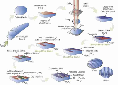
As shown in Figure 3, in a very simplified way (more details here), chips are made from a base of pure, perfectly polished silicon crystal, in the shape of a wafer about 200 nm in diameter. Layers of material, usually oxides, are then deposited on the silicon wafer, followed by a layer of photoresist. The wafer is then exposed to a laser, i.e. a controlled beam of light projected through a lens, to pattern the desired integrated circuit on the resin.
The role of photoresist and laser in etching
The circuit is then etched by removing part of the photoresist and oxide layer to print the desired pattern. A very small quantity of charged particles is then applied to the surface to create different zones of semiconductor material. The unwanted photoresist layers are then stripped away and metal wires are deposited on the wafer to connect the transistors together. This stage involves a further ten or so photoresist-laser-etch cycles. The chips are built layer by layer, repeating the operation between 40 and 100 times to obtain a complex integrated circuit. Once the processing cycle is complete, the wafers are cut into individual chips, tested and then encapsulated in protective cases.
Etching fineness: technological and environmental stakes
It is the resolution of the laser, determined by the wavelength of the light source, that determines the semiconductor’s nodes size(technology node). This unit of measurement (in nanometres), which originally referred to the length of the transistor gate, no longer corresponds to a physical measurement but is used to designate a certain generation of chip etching technology and the associated performance. The fineness of the laser engraving influences the density of transistors and therefore the amount of information that can be processed for a given surface area of integrated circuit. A smaller node indicates a more powerful and energy-efficient processor.
Environmental impacts of microchips: CO₂ emissions and water consumption
As we have seen, chip manufacture is based on particularly complex processes. The microelectronics industry is increasingly studying and considering the environmental impacts associated with the various stages of manufacture. Various groups of researchers and manufacturers are tackling the issue of the environmental impact of chips. In Europe, Imec (Interuniversity Microelectronics Centre) is the largest independent research and innovation center for nanoelectronics and digital technologies. Founded in 1984 and based in Belgium, the organisation's aim is to make semiconductors not only more energy-efficient but also more responsible. They provide a partly public tool for estimating the environmental impact of chip manufacture by node (imec.netzero).
CO₂ emissions by technology and scope (figure 4)
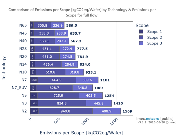
The growing impact of the smallest nodes
Figure 4 is taken from the public version of the netzero.imec tool. It shows the greenhouse gas (GHG) emissions in kg of CO₂ equivalents of 12 types of node (from the oldest at the top to the most recent at the bottom), according to the technology used (engraving fineness) and the scopes defined by the BGES methodology. Emissions increase with the engraving finesse, mainly due to the increase in the number of manufacturing steps for the smallest nodes. We can also see that for all the chips, Scope 2 accounts for the majority of the impacts. This is due to the very energy-intensive machines and processes used. In addition, most of the semiconductor industry is located in South and East Asia, where electricity is highly carbon-intensive.
Water consumption and resource tensions in Taiwan
The manufacture of chips also generates other types of environmental impact. For example, the cleaning stages require large quantities of very pure water, a resource that is already relatively scarce in Taiwan. As a result, during a particularly intense drought in 2021, the irrigation of a quarter of the country's rice fields was suspended in favour of the chip factories (Reporterre). Similarly, the silicon used for wafers must be extremely pure (99.99999999%), which involves complex purification stages that are costly in terms of energy and resources.
How to limit these impacts ? Solutions and best practises
Transitioning to low-carbon intensive electricity: challenges and opportunities
On the manufacturing side, switching to less carbon-intensive electricity would make it possible to reduce the GHG emissions associated with chips, through the use of renewable energies for example. But putting this into practice remains a complex task, given that Taiwan is the world's main supplier of chips. The country will need to speed up its transition to renewable energies if it is to produce enough to meet its climate targets. The subject is covered in detail in this scientific article.
Greenhouse gas abatement in factories
In the processes themselves, certain practices also make it possible to limit GHG emissions, such as abatement. The gases used are never completely consumed, and may be toxic, flammable or have a high global warming potential. Air pollution regulations in each country therefore require hazardous gases to be treated before they are released, by trapping them, burning them or using chemical reactions (e.g. TSMC). Extending this practice to all gases likely to have a major impact on the climate would make it possible to limit the impact of this industry.
Extending the lifespan of microchips: refurbishment and circular economy
Once the chips have been manufactured, the greatest lever for offsetting their environmental impact is to extend their lifespan. For smartphones and computers, this can involve reconditioning the equipment to give it a second life, as is. But it can also mean separating components from old equipment and reusing certain parts to reassemble a new device that meets a specific need.
The case of Citronics and micro computers
This circular model is beginning to emerge, with players such as Citronics, for example, which recovers processors from old telephones to make microcomputers, which are then used for automation or in the energy sector.
Supply challenges and dependence on Asian countries
Taiwan and South Korea’s dominance in global production
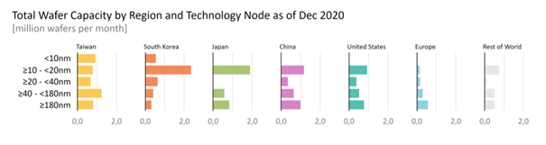
As mentioned above, South-East Asia accounts for the majority of the world's processor production, with nearly $300 billion of the $525 billion market in 2023. In terms of the number of production sites, East Asia accounts for 66% of the world's sites, with Taiwan producing 60% of the world's semiconductors and 90% of the most advanced logic chips. And Korean companies hold a dominant 60% share of the memory chip market.
Why are Europe and the US lagging behind ?
Europe lacks cutting-edge facilities in this field. Although it is home to several relatively advanced sites (STMicroelectronics, GlobalFoundries), most of its production (almost 50%) represents relatively old technologies (180nm nodes and wider), intended for use in industry and the automotive sector. More advanced technologies, for use in mobile phones or high-end computers, for example, are produced very little in Europe. The United States, on the other hand, have a good production capacity for all types of technology down to 10nm. Only Taiwan and South Korea have the infrastructure required to produce the latest cutting-edge chips, with an etch fineness of less than 10nm (Figure 5).
Geopolitical and economic risks of this dependence
In conclusion, semiconductors are at the heart of new technologies. While innovations in manufacturing processes since the 1970s have made it possible to multiply the engraving finesse by a factor of 10,000, the environmental impacts associated with these components are also increasing. Whether in terms of climate change or water stress, the more advanced the technologies, the greater the impact, despite the optimisation of processes. The fact that most production is located in Asia means that there are two issues at stake.
What solutions for relocating part of the production?
Firstly, locating production sites in a region where the electricity mix has a lower environmental impact would make it possible to limit the pollution generated by the manufacture of these components. In addition, setting up state-of-the-art production sites in Europe would reduce dependence on South-East Asian countries. Planning the installation of such infrastructures in Europe, on a site where low-carbon energy and water are relatively abundant, would be one way of responding to these two issues. It is all the more necessary to reflect on this subject as new uses are emerging that require ever more computing power. For example, the manufacture of Nvidia's HGX H100 GPU has an impact on climate change of 1,312 kg CO₂ eq.